
Model of Metal-Oxide-Semiconductor Contact Characteristics and Carrier Impurity Concentration in Depletion and Oxide Regions
DOI:
https://doi.org/10.31957/jfp.v3i2.196Keywords:
Metal-Oxide-Semiconductor Contact, Carrier ConcentrationAbstract
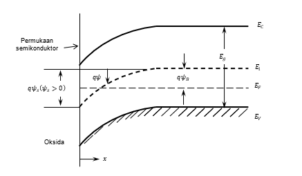
The aim of this research is to obtain characteristic modeling for forward and reverse voltages and the role of oxide as a barrier in the contact between metal semiconductors. When a forward or reverse voltage is applied, both types of semiconductor exhibit different characteristics. In this study, only these types are considered. The carrier concentration impurity within the semiconductor, width of the oxide material, depletion region, and active region are also reviewed. The method used was to examine the concept of a metal – oxide – semiconductor contact. In addition, the basic concept of energy bands is used to explain carrier flow events in semiconductors, which present band gaps, conduction band levels, and valence energy levels. The first research result is the characteristics of a metal – oxide – semiconductor-type connection when a negative and positive voltage is applied to a metal plate. The second is to find an equation for determining the concentration of substrate impurities. This equation shows the concentration of impurities in the semiconductor and the width of the oxide material, depletion region, and active region.
References
Mikelsten, D. (2019). Otomasi dan Teknologi Berkembang (Vol. 3). Cambridge Stanford Books.
Adhani, L., Aziz, I., Nurbayti, S., & Oktaviana, C. O. (2016). Pembuatan biodiesel dengan cara adsorpsi dan transesterifikasi dari minyak goreng bekas. Jurnal Kimia Valensi, 2(1), 71-80.
Cheng, D., et al. (2019). “Modeling of Metal-Oxide-Semiconductor Interface Characteristics.” Journal of Applied Physics, 125(12), 125101. DOI: 10.1063/1.5089661.
Syafira, N. W., Darlis, D., & Darlis, A. R. (2019). Perancangan Dan Implementasi Underwater Visible Light Communication (uvlc) Untuk Pengiriman Data Digital Menggunakan Filter Warna. eProceedings of Applied Science, 5(1).
Sutanto, H., & Wibowo, S. (2015). Semikonduktor Fotokatalis Seng Oksida dan Titania (Sintesis, Deposisi dan Aplikasi). Semarang: Telescope.
Sze, S. M., & Ng, K. K. (2007). Physics of Semiconductor Devices. John Wiley & Sons.
Nuryadin, B. W. (2020). Pengantar Fisika Nanomaterial: Teori dan Aplikasi.
Saktiawati, A. M. I. (2021). Diagnosis dan terapi tuberkulosis secara inhalasi. UGM PRESS.
Laksmiwati, A. M., & Suarya, P. (2017). Aktivasi Batu Padas dengan Asam dan Pemanfaatannya sebagai Penyerap Limbah Deterjen. Jurnal Media Sains, 1(1).
Pavlidis, D. (2015). Metal-Oxide-Semiconductor Devices: A Comprehensive Overview. Springer.
Pamuka, S. P., & Stefanie, A. (2023). Rancang Bangun dan Pengujian Sistem Energi Terbarukan Berbasis Tenaga Surya dengan Kapasitas 30 WP. JIM: Jurnal Ilmiah Mahasiswa Pendidikan Sejarah, 8(3), 1353-1360.
Fikri, R. (2023). Optimalisasi Keamanan Rumah dengan Implementasi Sistem Notifikasi Gerbang Cerdas Berbasis Internet of Things (IoT). Journal of Computer System and Informatics (JoSYC), 4(4), 816-829.
Kumar, A., & Kumar, R. (2020). “Impact of Impurity Concentration on the Electrical Characteristics of MOS Devices.” Materials Science in Semiconductor Processing, 117, 105284. DOI: 10.1016/j.mssp.2020.105284.
Baker, L. R., et al. (2018). Carrier Transport in Semiconductors: Theory and Applications. Wiley.
Ngaderman, H., & Sinaga, E. S. (2022). Model Karakteristik Kontak Logam Semikonduktor, Konsentrasi Muatan Dan Medan Listrik Di dalam Junction Logam Semikonduktor. Jurnal Fisika Papua, 1(2), 73–80. https://doi.org/10.31957/jfp.v1i2.10
Sutanto, H., Hidayanto, E., Nurhasanah, I., & Istadi, I. Pengaruh Laju Molar Mn Larutan Terhadap Mikrostruktur Lapisan Tipis GaN: Mn yang Dideposisi di atas Substrat Si Menggunakan Metode Sol-Gel. BERKALA FISIKA, 14(2), 63-70.
Grifiths D J. Introduction To Electrodynamics. Prentice Hall Of India Private Limited.
Halliday D, Resnick R dan Walker J. Fisika Jilid Dua Versi Diperluas. Binarupa Aksara.
Halliday, 1986. Fisika Jilid Dua. Airlangga
Jogiyanto H.M, 1998. Dasar-dasar Pemrograman Pascal. Andi Offset,Yogyakarta.
Krane Keneth S, 1992. Fisika Modern. John Wiley and Sons.
Ngaderman H, 2013. Efisiensi Maksimal Sel Surya p-n Junktion Berbasis Silikon. Universitas Cenderawasih.
Downloads
Published
Issue
Section
License
Copyright (c) 2024 This license allows reusers to distribute, remix, adapt, and build upon the material in any medium or format, so long as attribution is given to the creator.

This work is licensed under a Creative Commons Attribution-ShareAlike 4.0 International License.
![]()

